Menu Website

- Home
- MediaOutReach
- PolyU develops quantum-tunnelling field-effect transistor to overcome barriers to integrated-circuit chip development

PolyU develops quantum-tunnelling field-effect transistor to overcome barriers to integrated-circuit chip development
Senin, 31 Agustus 2026 | 21:53
Link berita berhasil disalin!
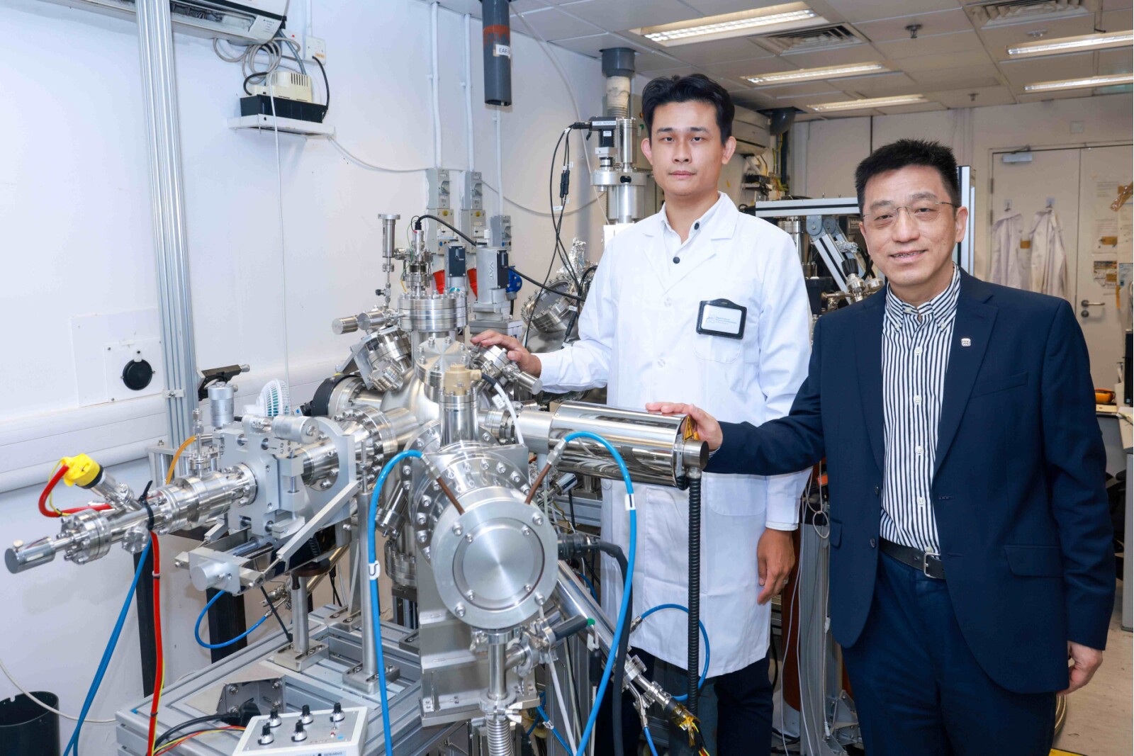
Prof. Jianhua Hao (right), Dr. Zehan Wu, Research Assistant Professor of Department of Physics and Materials at PolyU and the first author of the Research Article in Science (left), and the research team, fabricated ultra-thin heterostructure of 2D bismuth and indium selenide layers using pulsed laser deposition.
HONG KONG SAR -
Media OutReach Newswire
- 31 August 2026 - The next generation of microelectronics relies on
improvements in transistor switching performance to advance computing
power. However, conventional semiconductor technology has hit the
physical "Boltzmann limit", which restricts the energy efficiency of
traditional transistors. A research team at The Hong Kong Polytechnic
University (PolyU) has engineered a novel tunnelling field-effect
transistor (TFET) utilising 2D nanomaterials. The breakthrough can offer
the fundamentals for energy-efficient computing and next-generation AI
chips.
The research was led by Prof. Jianhua HAO, Head of the Department of Physics and Materials and Chair Professor of Materials Physics and Devices at PolyU, in collaboration with the National University of Singapore, The Hong Kong University of Science and Technology, Peking University, and the Singapore University of Technology and Design. The findings have been published in the prestigious scientific journal Science.
Conventional transistors rely on thermionic emission of electrical charges, which requires a minimum gating voltage of 60 millivolts (mV). However, the "Boltzmann limit" makes subthreshold swing values below 60 mV decade⁻¹ at room temperature physically impossible, limiting progress in high-performance electronics.
Prof. Hao said, "By adopting quantum tunnelling, our TFET breaks through this boundary, paving the way for ultra-low-power, high-performance integrated circuits essential for emerging AI chips and advanced semiconductor applications."
Prof. Hao's team created ultra-thin heterostructure of 2D bismuth and indium selenide alternating layers using pulsed laser deposition. By exercising precise control over the layer structure, the normally semi-metallic bismuth transforms into a semiconductor in 2D form, allowing charge carriers to tunnel efficiently into indium selenide through quantum tunnelling mechanism.
The resulting TFET achieved SS values well below the 60 mV decade⁻¹ limit. Operating at room temperature on silicon substrates, the device required a gate-voltage range of only 160 mV-far lower than the 800 mV originally required.
The device resolved a challenge in experimental TFETs by delivering a high output current alongside an exceptionally high ON/OFF current ratio, which helps drive multiple downstream logic gates and diminish circuit-delay.
The research was led by Prof. Jianhua HAO, Head of the Department of Physics and Materials and Chair Professor of Materials Physics and Devices at PolyU, in collaboration with the National University of Singapore, The Hong Kong University of Science and Technology, Peking University, and the Singapore University of Technology and Design. The findings have been published in the prestigious scientific journal Science.
Conventional transistors rely on thermionic emission of electrical charges, which requires a minimum gating voltage of 60 millivolts (mV). However, the "Boltzmann limit" makes subthreshold swing values below 60 mV decade⁻¹ at room temperature physically impossible, limiting progress in high-performance electronics.
Prof. Hao said, "By adopting quantum tunnelling, our TFET breaks through this boundary, paving the way for ultra-low-power, high-performance integrated circuits essential for emerging AI chips and advanced semiconductor applications."
Prof. Hao's team created ultra-thin heterostructure of 2D bismuth and indium selenide alternating layers using pulsed laser deposition. By exercising precise control over the layer structure, the normally semi-metallic bismuth transforms into a semiconductor in 2D form, allowing charge carriers to tunnel efficiently into indium selenide through quantum tunnelling mechanism.
The resulting TFET achieved SS values well below the 60 mV decade⁻¹ limit. Operating at room temperature on silicon substrates, the device required a gate-voltage range of only 160 mV-far lower than the 800 mV originally required.
The device resolved a challenge in experimental TFETs by delivering a high output current alongside an exceptionally high ON/OFF current ratio, which helps drive multiple downstream logic gates and diminish circuit-delay.
📢 Publisir Berita & Kegiatan Instansi Anda di RiauGreen
Jangkau pembaca luas & terindeks Google News. Pilih paket rilis pers, advertorial, atau kemitraan media.
BERITA LAINNYA

Senin, 31 Agustus 2026 | 21:56

Senin, 31 Agustus 2026 | 21:55

Senin, 31 Agustus 2026 | 21:54
Senin, 31 Agustus 2026 | 21:54
Senin, 31 Agustus 2026 | 21:53

Senin, 31 Agustus 2026 | 21:52

Senin, 31 Agustus 2026 | 21:52

Senin, 31 Agustus 2026 | 21:51
Senin, 31 Agustus 2026 | 21:49
Senin, 31 Agustus 2026 | 21:48

Senin, 31 Agustus 2026 | 11:36
BERIKAN KOMENTAR


-

-
Senin, 31 Agustus 2026 | 21:56
Hong Kong Science and Technology Parks Corporation Kicks Off 25th Anniversary Prelude "Innovation. Next by Nature."
-
Senin, 31 Agustus 2026 | 21:55
Five Years After Expansion, Qianhai Opens a New Chapter in Institutional Opening-Up
-
Senin, 31 Agustus 2026 | 21:54
Over 20,000 Young Players Chase Their Dreams on the Pitch - Beijing's Very Own "World Cup" Concludes
-
Senin, 31 Agustus 2026 | 21:54
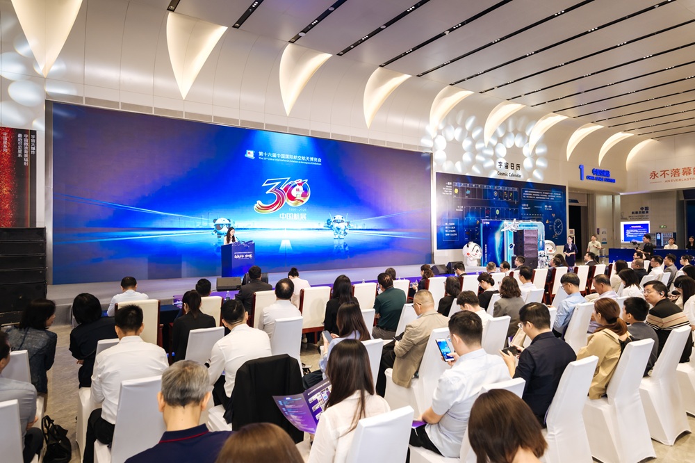
Airshow China kicks off its 100-day countdown to the 30th Anniversary
-
Senin, 31 Agustus 2026 | 21:53
PolyU develops quantum-tunnelling field-effect transistor to overcome barriers to integrated-circuit chip development

-

-
 Selasa, 25 Agustus 2026 | 20:09
HIS Implementasikan B50, Perkuat Komitmen Mendukung Ketahanan Energi Indonesia
-
 Selasa, 25 Agustus 2026 | 20:10
Duiba Group Announces Rapid Scaling of AI Short Drama Business and Significant AI Technology-Driven Revenue Growth
-
 Selasa, 25 Agustus 2026 | 20:08
Waskita Beton Precast Bersama PMI Salurkan Bantuan Kemanusiaan untuk Masyarakat Terdampak di NTT
-
 Selasa, 25 Agustus 2026 | 20:12
FOPLP Curing and Annealing Oven Adds Dedicated 310mm Chamber Configuration
-