Menu Website

- Home
- MediaOutReach
- Toray Engineering: Launch of UC5000 Semiconductor Packaging Equipment Compatible with Large Glass Panels

Toray Engineering: Launch of UC5000 Semiconductor Packaging Equipment Compatible with Large Glass Panels
Jumat, 28 Maret 2025 | 10:35
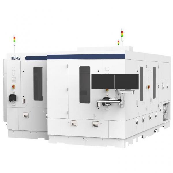
PLP-compatible bonder UC5000
TOKYO, JAPAN -
Media OutReach Newswire
- 27 March 2025 - Toray Engineering Co., Ltd.,has developed the UC5000,
a high-accuracy semiconductor packaging equipment (bonder) for panel
level packaging "PLP". PLP is an advanced semiconductor packaging
technology, for which there is growing demand particularly from AI
servers. Sales of the UC5000 will commence in April 2025.
This system is capable of packaging chips with a high accuracy of ±0.8μm using thermal compression bonding "TCB" on 515mm × 510mm and 600mm × 600mm panels complying with the SEMI Standards. It can also carry out high-accuracy TCB packaging on glass panels, which is gaining attention as an alternative material to silicon, contributing to the manufacturing of next-generation semiconductor packaging.
Toray Engineering aims to supply the UC5000 to manufacturers of semiconductors, targeting 3 billion yen in orders in FY2025 and 10 billion yen in FY2030.
With the increasing performance of semiconductors, chiplets—a technology that packages several semiconductors chips into a single package, as represented by 2.5D packaging—is gaining attention. Wafer level packaging based on silicon wafers, such as those using interposers for high-speed transmission between semiconductor chips, was the mainstream for semiconductor packages comprising such chiplets. Going forward, with semiconductor packages becoming bigger due to increasing performance, PLP based on glass panels, which allow sizes larger than wafers and rectangular shapes, is gaining attention because wafers cannot grow larger in size and have poor manufacturing efficiency, having to cut rectangular shapes from round wafers.
However, compared to wafers, large glass panels warp significantly and are difficult to transfer, and require larger heaters to heat the panels. There were thus issues with heat control within system as well as difficulties in achieving high-accuracy packaging while taking into account the expansion and shrinking of materials due to heat.
The UC5000 achieves high-accuracy packaging of ±0.8μm on large panels and TCB through: a technology—used in TCB packaging equipment for small substrates, for which Toray Engineering has a mass production track record at least 100 units so far—that maintains accurate packaging, calibrating for impact from heat arising from high temperatures of 300℃ and higher during soldering; high-accuracy packaging technology and panel-warping correction transfer technology that were used in systems equipped with bridge chips for large panels, for which there is a mass production track record of at least 50 units; and a complete overhaul of the core control system for use in the UC5000. This system is also compatible with front-opening unified pods (FOUPs) for panels and tape frames that comply with SEMI Standards, which are starting to be adopted in the downstream processes of semiconductors, and its composition can also handle mass production at the latest plants.
Besides the TRENG coater and large glass substrate inspection system, Toray Engineering will contribute to the further adoption of PLP by adding the UC5000 to the lineup for the field of advanced semiconductor packaging.
For more information, please visit www.toray-eng.com.
BERITA LAINNYA

Sabtu, 29 Maret 2025 | 10:06

Sabtu, 29 Maret 2025 | 10:05
Sabtu, 29 Maret 2025 | 10:04
Sabtu, 29 Maret 2025 | 10:03


Sabtu, 29 Maret 2025 | 09:58

Jumat, 28 Maret 2025 | 14:03
Jumat, 28 Maret 2025 | 14:03

Jumat, 28 Maret 2025 | 10:43


BERIKAN KOMENTAR


-
 Minggu, 30 Maret 2025 | 19:43
Azwar Siswa Lemdiklat Setukpa Polri Angkatan 54 Berbagi Sembako Kepada Masyarakat Rohil
-
 Minggu, 30 Maret 2025 | 19:43
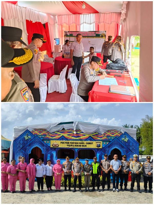
Kapolres Rohil Bersama Bhayangkari Kunjungi Pospam IdulFitri Simpang Martabak, Utamakan Pemudik Aman - Nyaman
-
Minggu, 30 Maret 2025 | 12:24
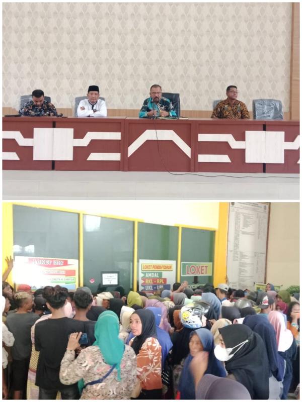
Aktivis Pendidikan Desak Pemprov Riau Bayarkan Ratusan Gaji Guru Honorer Dikdas
-
 Sabtu, 29 Maret 2025 | 23:21
Peduli Masyarakat Sekitar, Apical Gelar Buka Puasa Bersama dan Santunan Anak Yatim di Dumai
-
 Sabtu, 29 Maret 2025 | 22:13
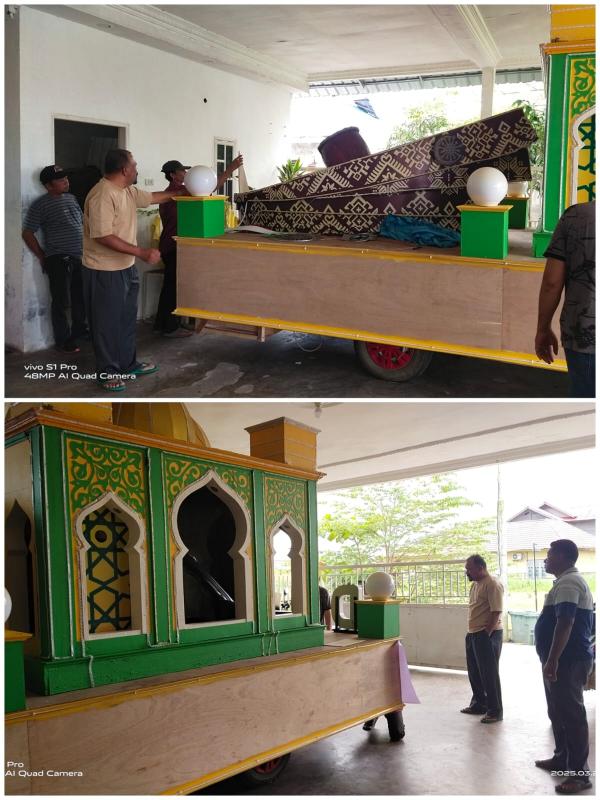
Meriahkan Hari Raya IdulFitri Tahun Ini, DLH Rohil Usung Tema Miniatur Masjid dan Tanjak
-
 Sabtu, 29 Maret 2025 | 21:25
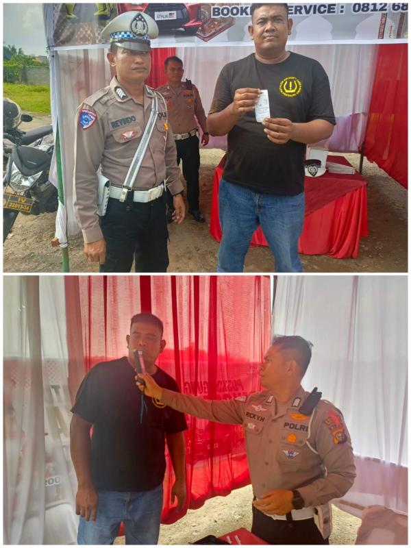
Kasatlantas Polres Rohil Pimpin Tes Kadar Alkohol Para Supir Angkutan Umum

-
 Sabtu, 29 Maret 2025 | 12:21
Calla Pramuka Link Download Jadi Keyword yang Sering Dicari Netizen di Internet
-
 Sabtu, 29 Maret 2025 | 13:14
Video Viral Lisa Mariana Ini telah Ditonton oleh Ratusan Ribu Kali, Cek Link Disini
-

-
 Kamis, 27 Maret 2025 | 21:17
Gaji Cair 2 Bulan, DLH Rohil Sampaikan Ucapan Terimakasih Kepada Bupati dan Wakil Bupati
-
 Sabtu, 29 Maret 2025 | 13:18
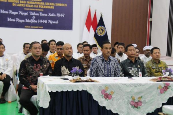
Lapas Kelas IIA Pekanbaru Berikan Remisi Idul Fitri dan Nyepi kepada 1.050 Napi
-
 Jumat, 28 Maret 2025 | 14:14
Rhenus Group Perluas Dewan Eksekutifnya, Menyambut Anggota Baru untuk Mendukung Transformasi dan Pertumbuhan Grup